Architecture

Perpendicular lines create a shared array current.

Voltage DACs drive the bit-lines while each source-line current passes through a transimpedance amplifier and ADC. The sensing resistance connects the analog array to the available conversion range.

Crossbar operation

The design variable sits between the array and ADC.

Bit-lines (BLs) run perpendicular to source-lines (SLs), with a 1T1R bitcell at each crossing. DACs drive the BLs, and the TIA on each SL holds the line at VDC. Activating M word-lines computes an M × N matrix-vector multiplication in one step.
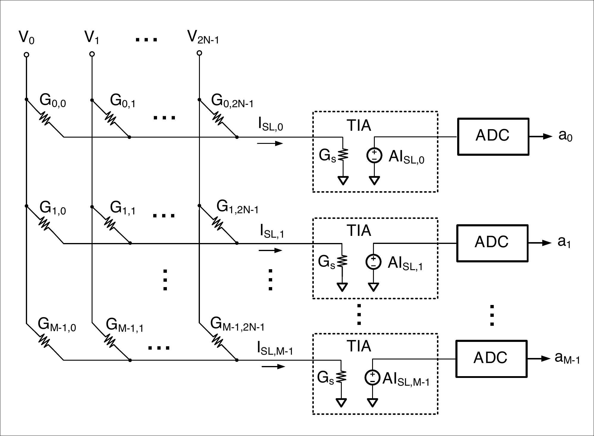
  • Signal path. Rs, the TIA input impedance, scales the SL current reaching the ADC.
  • Noise path. DAC mismatch, bitcell variation, ADC clipping, and ADC quantization.
  • Design target. The Rs that maximizes compute SNR for the chosen device and N.
Voltage-driven resistive crossbar with perpendicular input columns, source-line current sensing, transimpedance amplifiers, and ADCs.
Crossbar architecture. Perpendicular bit-lines and source-lines feed one TIA and ADC per output source line. Adapted from Fig. 1(a) of the ISCAS 2022 paper.

Weight encoding

Complementary columns remove the zero-input current.

Finite Ron and Roff leave a current even at a zero dot product. Differential encoding removes it: adjacent columns receive opposite-sign inputs, and a bitcell pair stores one ternary weight. An N-term dot product therefore occupies 2N physical columns.

b2k=1,if G2k−1>G2k0,if G2k−1=G2k−1,if G2k−1<G2k
Ternary weight stored in a bitcell pair. Eq. (1) of the paper.

Signal model

Only a fraction of the ideal current reaches the readout.

Rs appears in parallel with the array resistance Rarr, so the SL delivers only a fraction SI of the ideal current. Since Rarr ∝ 1/N, a longer dot product shrinks the signal, and lowering Rs recovers it. However, an Rs below about 500 Ω carries significant area overhead.

Isig=RarrRarr+Rs∑k=1NV2kΔG2k=SIIideal
Signal current on the SL. Eq. (2) of the paper.
Rarr=1∑j=12NGj,SI=RarrRarr+Rs
Array resistance and current scaling factor. Eq. (3) of the paper.

Noise model

Four non-idealities corrupt the source-line current.

ISL=Isig+Inb+Ind+Inc+Inq
SL current with its four noise terms. Eq. (4) of the paper.
1Inb · Array

Bitcell variation

Gon and Goff vary across the array, modeled with a 4% standard-deviation-to-mean ratio.

2Ind · Drivers

Input-DAC mismatch

DAC finger mismatch adds noise that grows with the input, modeled at 4% per finger.

3Inc · ADC

Clipping

SL current beyond ±Iclip = ±2 µA saturates at the ADC rail.

4Inq · ADC

Quantization

A BADC-bit ADC adds uniform noise over one step of the clipping range.
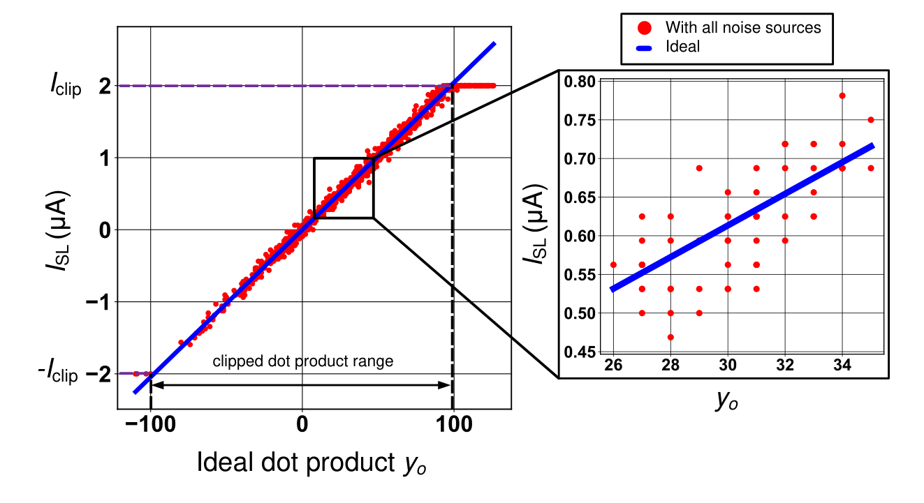
Source-line current versus ideal dot product for a ReRAM crossbar, showing clipping at plus and minus two microamperes and an inset of noisy samples scattered around the ideal line.
Noise on the SL current. ReRAM, N = 512, Rs = 316 Ω, 6 b ADC. Adapted from Fig. 1(b) of the ISCAS 2022 paper.

Compute SNR

Noise pushes ADC outputs off the ideal line.

Currents beyond ±Iclip collapse onto the rails, and the remaining noise scatters samples around the ideal line. Compute SNR compares the signal power with the total power of the four noise terms.

SNR=E[Isig2]E[Inb2]+E[Ind2]+E[Inc2]+E[Inq2]
Compute SNR at the SL. Eq. (5) of the paper.

Model boundary

The limits hold under stated assumptions.

The reported limits are conditional on these assumptions and the evaluation parameters.

  • Binary devices. Each device takes only the states Ron and Roff.
  • Sensing. Rs equals the TIA input impedance.
  • Circuit check. The behavioral models were validated against 22 nm SPICE simulation.
  • Parasitics. The paper's equation omits wire parasitics. The Architect adds them with a full network model.